Our Technology
Introduction to the Plasma Jet Technology
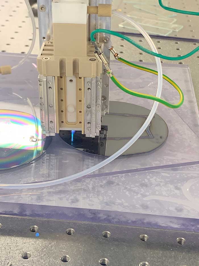
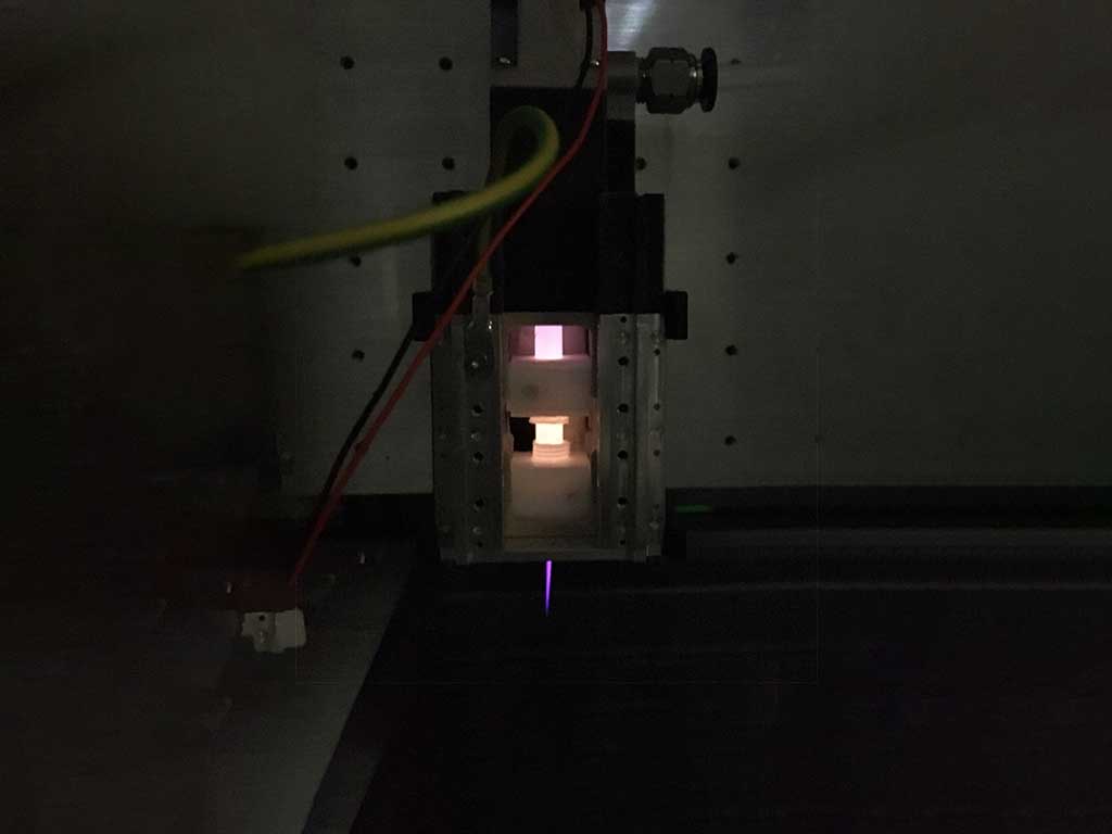
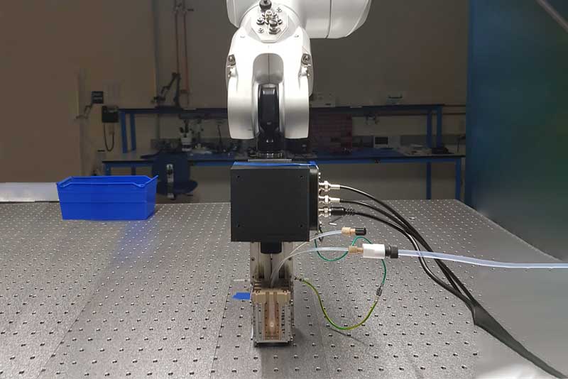
Plasma jet printer for additive printed electronics manufacturing comprises a patent protected plasma print head with an integrated fluid delivery system.
The material to be printed is aerosolized and introduced into the print head where a plasma is generated. The electromagnetic field that generates the gaseous plasma discharge accelerates the aerosolized ink towards the print head. As the aerosolized ink passes through the plasma discharge, the reactive ionic species, electrons and free radicals generated in the plasma interact with the ink and by controlling the nature of these plasma species (oxidizing, reducing etc.,), the electronic properties of the aerosolized ink can be tailored in-situ.
Instead of a wet chemical process that tailors the material properties of the ink, a dry plasma process is used to tailor the material properties in-situ printing eliminating the need for both pre-processing of ink and post processing of printed pattern
Why Plasma Technology?
Challenges with Contemporary Technologies
The commercialization of high value, printed electronics products relies on a major manufacturing bottleneck of multi-material printing of conductors and dielectrics. The current process requires multiple steps and high quality ink supply. State of the art technologies for additive manufacturing of electronics rely heavily on ink quality and low temperature curing of printed patterns. Nanoparticle inks are primarily being explored, however retaining the nanoparticle size, shape, oxidation state, uniform dispersion, preventing aggregation etc., require complex wet chemical processing. Curing the printed pattern at low temperature is a challenge as high temperature curing shall induce oxidation. Additionally, building up of the aspect ratio is challenging and will inevitably result in a sandwich layer, if printing and curing is done repeatedly.
Patents Granted:
U.S. Patent No. 10,991,548 B2 ; US Patent No. 10,995, 406 B2 ; US Patent No. 11,241,833 B2
- Gandhiraman et al., Modular Print Head Assembly for Plasma Jet Printing. Patent No.: US 10,991,548 B2;
- Gandhiraman et al., In situ Tailoring of Material Properties in 3D Printed Electronics. Patent No.: 10,995,406 B2;
- Gandhiraman et al., 3D Printed Electronics Using Directional Plasma Jet. Granted. US Patent No. : 11,241,833 B2
- Several patents and PCTs filed
USPs of our Patented Plasma Technology
Plasma process is widely used in semiconductor industry for chip manufacturing. Plasma is an electrically conducting gaseous discharge that can be used to tailor the material properties. Unlike the semiconductor industry that uses low pressure (Vacuum) plasma, our technology is based on atmospheric pressure plasma.
- Having the ability to tailor the material properties in gas phase, plasma offers an environmentally friendly process that does not leave behind liquid industrial waste or toxic byproducts.
- As the material properties can be tailored in the gas phase at the print head, plasma jet printing takes unprocessed, low grate ink and uses in-situ plasma process to print high quality materials.
- Need for heavy chemical processing of copper/metal inks normally required in state of the art copper printing technologies is eliminated with the nanoparticle free approach.
- Being a dry process, the plasma jet printing procedure does not require a curing step. This is a major step in both environmental and user safety, as the ink synthesis is simple and does not rely on heavy chemical synthesis steps.
- With a heavy focus on plasma process for printing and less reliance on the ink supply chain makes this a viable technology for cost effective manufacturing
List of Publications:
- Ramamurti et al., “Atmospheric Pressure Plasma Printing of Nanomaterials for IoT Applications” IEEE Open Journal of Nanotechnology, 2020, 1, 47-56.
- Dey et al., “Plasma jet deposition and in-situ reduction of highly acidic graphene oxide”. ACS Nano 2018, 12 (6), 5473.
- Dey, A. Et al., “Plasma jet based in-situ reduction of copper oxide in direct write printing”. Journal of Vacuum Science and Technology B, 2019, 37, 031203.
- Ram P. Gandhiraman et al., “Plasma Jet Printing for Flexible Substrates”. Applied Physics Letters. 2016, 108, 123103.
- Ram P. Gandhiraman et al., “Plasma Jet Printing of Electronic Materials on Flexible and Non-Conformal Objects”. ACS Appl Mater Interfaces. 2014, 6, 20860.
- Ram P. Gandhiraman et al., “Scalable Low-Cost Fabrication of Disposable Paper Sensors for DNA Detection”. ACS Appl Mater Interfaces. 2014, 6, 22751.